Bipolar Junction Transistor - Summary
ECE 4339
Han Q. Le
(copyrighted) U. of Houston
Calculation package
0. Overview and Summary
In the following, we will see illustration
calculation for the following key aspects of the BJT:
a- Behavior of majority carrier in the base - in this example,
holes.
b- The effect of long base (carriers die off) vs. short base
(carriers transferred to collector)
c- Minority carriers in the emitter (in this case, electrons): the
important of long emitter vs. short emitter.
d- Effects of asymmetric doping: heavy for emitter and light
(relatively) for base.
e- Overall carrier behavior and currents
f- The I-V curve of BJT
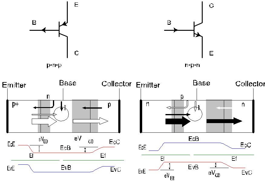
In the follow, we will consider pnp structure. And we will consider only steady state (no explicit time-dependence).
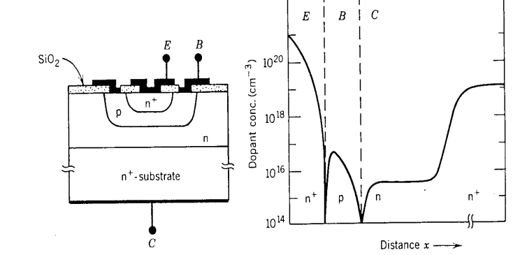
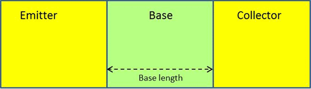
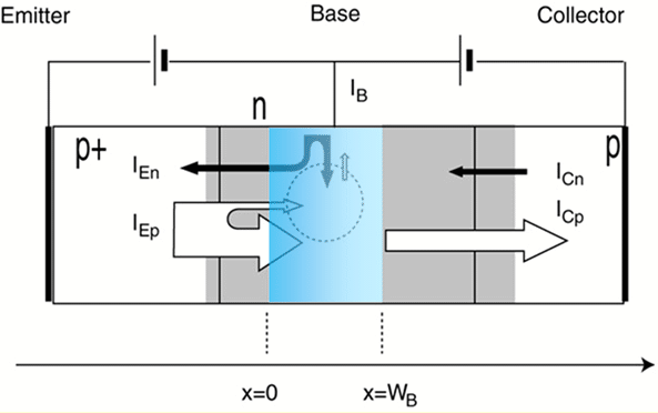
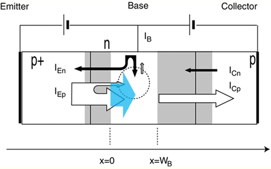
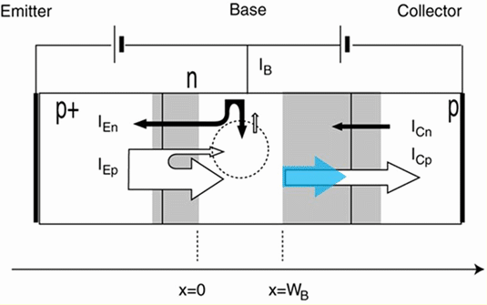
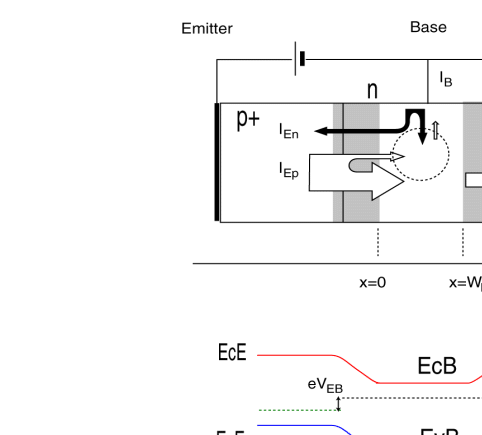
1. Basic structure
Band structure with bias
2. Hole distribution and diffusion current in the base (PNP)
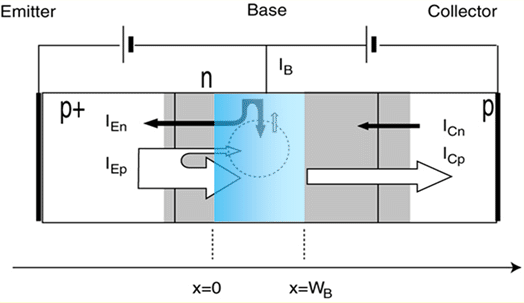
2.1 Discussion
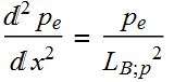
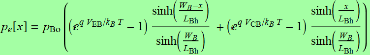
To find the distribution of holes in the base, we solve the DE for excess carriers in the base.
Mathematical details
First, we set up to solve the differential equation
![]()
One difference from previous exercises we did with p-n junction diode is that we treated each side of the diode as infinite. Here we notice is that this is a finite section, hence we keep both terms.
Next, we set up the boundary condition.
At x=0: left side of the base (start from the E-B depletion
boundary), the excess hole concentration has to be the excess
carriers (see Chapter 5, section
3.2):
![]()
At x=![]() :
right side of the base (at the C-B depletion boundary), the excess
hole concentration has to be the excess carriers:
:
right side of the base (at the C-B depletion boundary), the excess
hole concentration has to be the excess carriers:
![]()
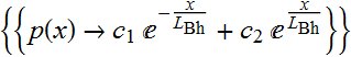
Applying boundary condition:
![]()
![]()
![]()
![]()

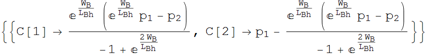
We now substitute the coefficients into the solution:
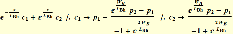
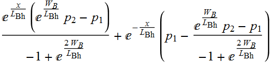
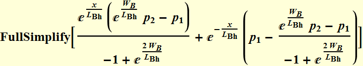
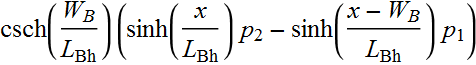
Or we can write: The excess hole concentration in
the base is:
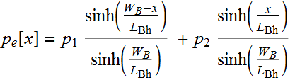
Full expression:
2.2 Hole distribution in base
The following is a function of the hole distribution in the base

Plot the hole distribution in base
The above calculation is an approximation that ignores the variation of the depletion regions in the base as a function of the the bias voltages. But it is useful and illustrative.
Exercise: plot hole distribution in base as a function of increasing emitter-base bias (forward). Use Si parameters to calculate
Exercise: Comparing long base vs short base
relative to diffusion length (Vice versa, long vs. short ![]() ). Discuss
). Discuss
2.3 Diffusion current
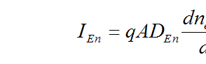
2.3.1 Holes diffusing current from emitter to base
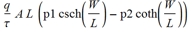
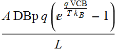
It is given by: (note the sign - here q is positive for holes)
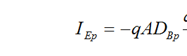
But we already know the hole distribution in the base

Taking the derivative:
![]()
At the emitter-base junction, x=0
Therefore, the emitter to base hole
diffusion current is:
or:
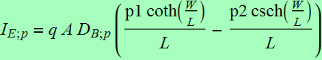
![]()
We can substitute ![]()

For a full expression:

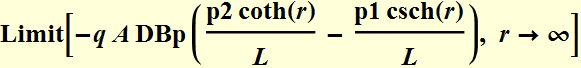
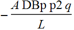
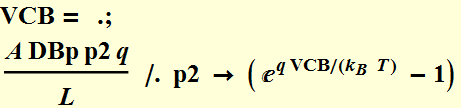
2.3.2 Limiting case: very large base: decoupled diode
Let’s check if this gives the known answer if the base length is infinite.
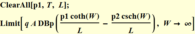
This is the (ideal) equation of diode: in other words, if the baselength is infinite, the emitter-base current is essentially the ideal diode current. This confirms we have the correct limit.
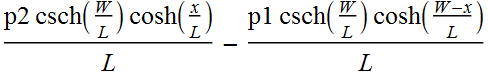
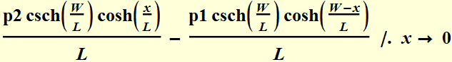
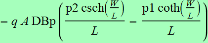
2.3.3 Current of holes diffusing from base to collector
Now, let’s check the hole diffusion current from base to collector.
The current is: (q is positive for holes)
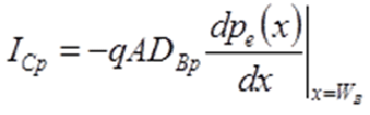
![]()
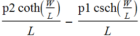
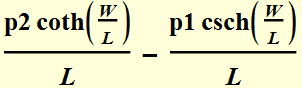
Hence: 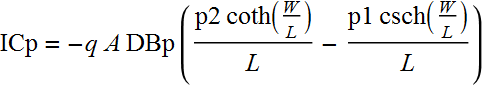
or, we can substitute ![]()

For a full expression:

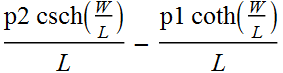
2.3.4 Limiting case: very large base - decoupled diode - Base-Collector current
Again, if the baselength is infinite, the base-collector current is essentially the diode current also, just as expected.
2.3.5 Holes diffusion current in Base
Let's take a look at emitter-base hole current (blue) and the base-collector current (red) as a function of base length for different emitter-base voltage:
Plot the hole diffusion current in Base
Exercise discussion: What do those graphs tell us?
2.4 Overall holes behavior
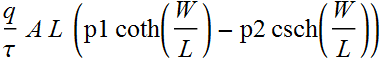
2.5 Base transport factor
2.5.1 Discussion
From the above
results, the base transport factor is:

If we approximate by dropping ![]() since it is much smaller than
since it is much smaller than ![]() ,
then:
,
then:
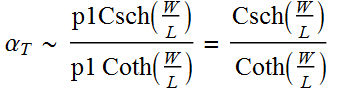
Or: 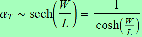 .
.
Clearly, we want  or the base to be much shorter than the majority carrier diffusion
length.
or the base to be much shorter than the majority carrier diffusion
length.
2.5.2 Illustration
We can see how the base transport factor depend on the base width:
Base transport factor
It's clear that the shorter the base, the better is the base transport factor
Below, we will see how base transport factor as a function of transitor bias voltage:
Although this approximation is not very good for small bias voltage, the qualitative behavior is correct in the plot above: There must be some finite bias voltage between emitter-collector (transistor turned on) for the base transport factor to be reach its value. This intuitively makes sense, doesn't it? If you don't turn on the bias, (and hence, there is no current between emitter-collector) who cares what the transport factor is?
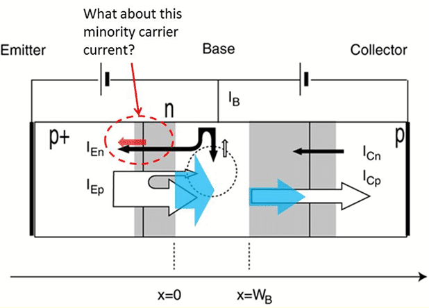
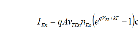
3. Electron distribution and diffusion current in emitter
For a transistor to be efficient, it is essential that the minority current, especially the electron current from base to transmitter to be very small compared with the hole current from emitter to base. Here, we'll see that doping and length of the emitter are crucial.

3.1 Discussion
For those electrons from the base going to the
emitter, the excess carrier density is (if we use the infinite
diode model):
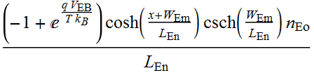
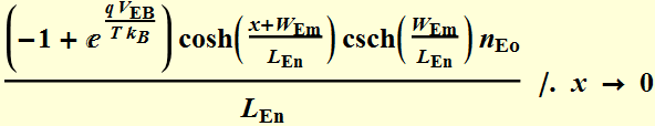
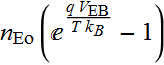
![]()
And the diffusion current is: (notice that the charge has a minus sign, and double minuses is a plus - it is the opposite if we consider NPN)
However, the above formula ![]() is
good only for the case we have infinitely long emitter. In
reality, it is not. Here, we must include the effect of finite
length emitter to be realistic.
is
good only for the case we have infinitely long emitter. In
reality, it is not. Here, we must include the effect of finite
length emitter to be realistic.
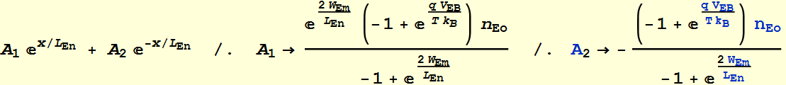
3.1.1 Mathematical consideration for finite-length emitter
For finite emitter length, we MUST solve the
diffusion equation with correct boundary condition:
![]()
![]()
![]()
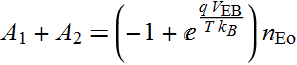
To determine A1 and A2, we apply the boundary condition: let x=0
![]()
![]()
Therefore:
![]()
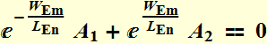
We apply the boundary condition at x=-![]() ,
where the excess electrons density should be zero for an ohmic
contact. (The collection of electrons at the electrical contact is
so efficient that there cannot be any excess carriers).
,
where the excess electrons density should be zero for an ohmic
contact. (The collection of electrons at the electrical contact is
so efficient that there cannot be any excess carriers).
An efficient sink will not have excess water.
![]()
![]()
Therefore we have the equation
![]()
Now we can solve for A1 and A2:

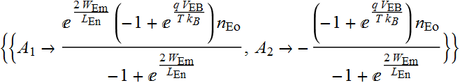
Now we substitute A1 and A2 in the equation:
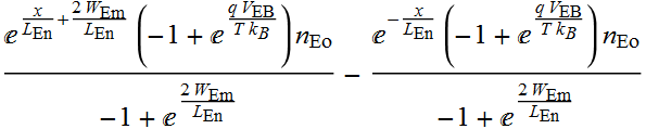
![]()
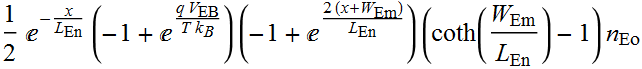
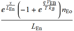
Now, we want to find the diffusion current by taking the gradient:
![]()

![]()
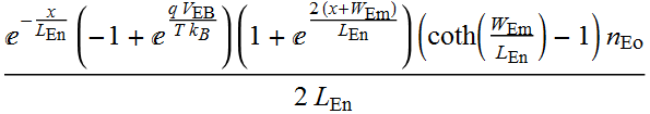
![]()

![]()

Finally, we have the solution, the gradient of excess carriers (electrons) in Emitter is:
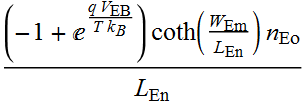
3.1.2 The minority current from Base to Emitter.

From the
gradient obtained above, the electron current in Emitter is:
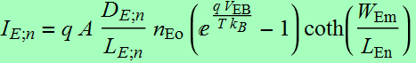
We define: 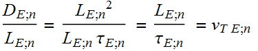 which is defined to be the
transit velocity. And we can write the electron current
in the emitter:
which is defined to be the
transit velocity. And we can write the electron current
in the emitter:
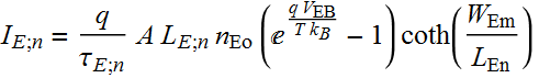
or:
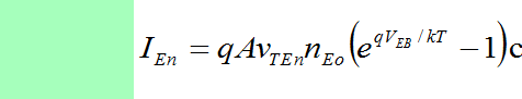
Let’s check the limiting result for a long emitter; The current is proportional to:
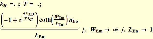
This is exactly the n-to-p electron diffusion
current of the ideal diode behavior.
Hence, the electron current from Base to Emitter is the electron
forward-bias diode current as expected.
Review p-n junction diode: how can we make this current be “small” compared with the hole forward-bias current from emitter to base? (See Chapter 5- part 1, section 3.2.2)
p-n junction diffusion currents - log scale
Review Chapter 5- part 1. If we have a symmetrically doped diode, where the electron current from n to p is as large as the hole current from p to n, then there will be very large recombination as the two populations meet each other! In a transistor, it is not desirable to have all the majority carriers from the emitter “eaten up” by the minority current coming from the base. Asymmetric doping is essential.
3.2 Electrons behavior in emitter
3.2.1 Base doping vs. emitter doping
Here, we'll see how important the relative doping between the emitter and the base is on the two types of current. Use the calculation module below, vary the doping concentration.
EB junction diffusion currents - log scale (manipulate doping concentrations)
Here, we will plot to compare the electron current
in the emitter from the base vs the hole current in the base from
the emitter. (think about export model) Left side: emitter ; Right side: base
(linear scale)
By manipulate the doping of emitter (a1) and base (d), we see that
we can make wrong choice if emitter doping is less than base
doping.
Left side: emitter ; Right side: base
Now we find out a reason for the large asymmetry in the emitter and base doping: emitter is usually heavily doped while the base is very lightly doped, that way, we electrons from base to the emitter won't "eat up" holes in the emitter (which is supposed to go to the collector)
3.2.2 Effects of emitter length
We use the same calculation module above, except here, we will manipulate Emitter length.
EB junction diffusion currents - log scale (manipulate Emitter length)
Manipulate the emitter length WEm. Do we want a
high electron current in the emitter?
Now we see an advantage of using long emitter: we have less
electron current from base to emitter.
Summarize 2 key factors with respect to E-B design to minimize the base-emitter electrons current for an efficient transistor.
To reduce the electron current from base to
emitter:
1- Use heavy emitter doping vs. very light base doping
2- Use long emitter length relative to electron diffusion length
3.3 Emitter efficiency summary
3.3.1 Summary of discussion
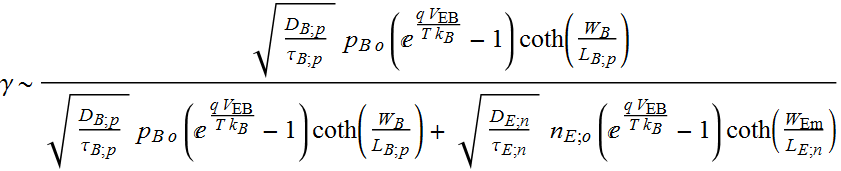
It is desirable to have high emitter efficiency γ,
which is defined as:
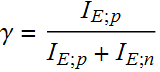
From the above results:
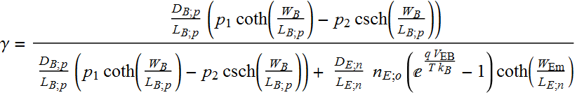
We can approximate by dropping ![]() :
:
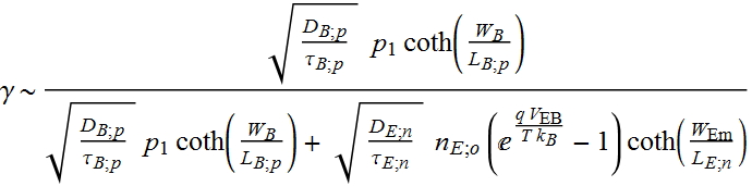
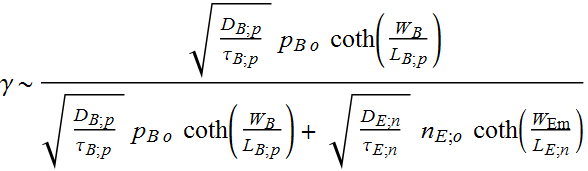
Hence the approximated emitter
efficiency is:
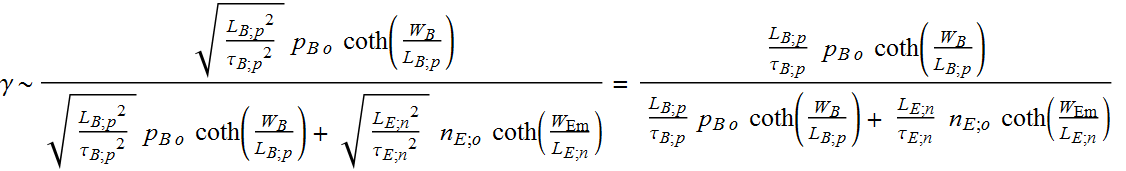
To have high emitter efficiency, we want ![]() .
Or:
.
Or:
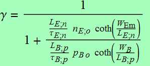
There are three parameters to be considered:
1- Transit velocity:  and
and  :
we can't do much with these, as they are determined mostly by the
intrinsic material properties.
:
we can't do much with these, as they are determined mostly by the
intrinsic material properties. 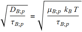 and
and 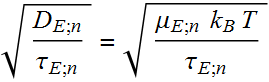 .
For the base, we can engineer the doping and material quality for
large hole mobility. But we also want long lifetime for large
diffusion length for high base transport factor. For emitter, we
want low mobility for short diffusion length, but we DON'T want
too poor conductivity (and high resistivity) in the emitter
either. Thus, there is not much room to engineer these
parameters.
.
For the base, we can engineer the doping and material quality for
large hole mobility. But we also want long lifetime for large
diffusion length for high base transport factor. For emitter, we
want low mobility for short diffusion length, but we DON'T want
too poor conductivity (and high resistivity) in the emitter
either. Thus, there is not much room to engineer these
parameters.
2- We can have ![]() :
As already discussed above, this is achieved by having the emitter
doped heavily compared with the base. In fact, this is the basic
design parameter of a BJT.
:
As already discussed above, this is achieved by having the emitter
doped heavily compared with the base. In fact, this is the basic
design parameter of a BJT.
3- We want 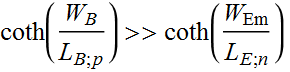 :
as discussed above: we want long emitter:
:
as discussed above: we want long emitter: 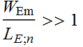 and short base:
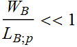
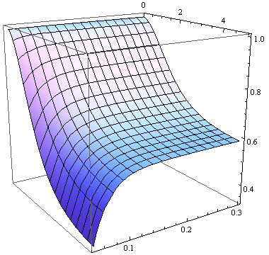
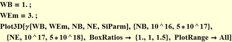
3.3.2 Illustration
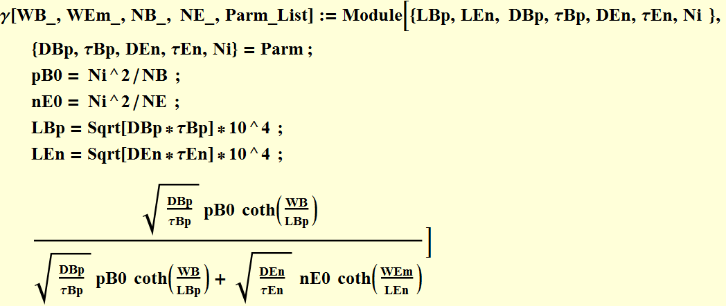
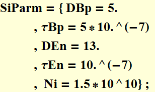
We will see how the base and emitter length affect the emitter efficiency in the following plot:
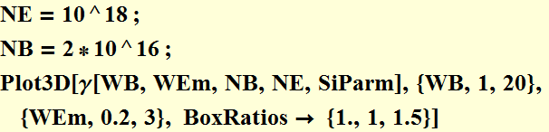
Notice that the best emitter efficiency is at the far corner: where base length is shortest and emitter length is longest. The nearest corner is the opposite: worst efficiency for short emitter and long base.
In the following plot, we will see how the base and emitter doping affect the emitter efficiency:
Notice the similarity with the case above. The best emitter efficiency is at the far corner, where base doping is lowest and emitter doping is highest. The nearest corner is the opposite: worst efficiency for low emitter doping and high base doping.
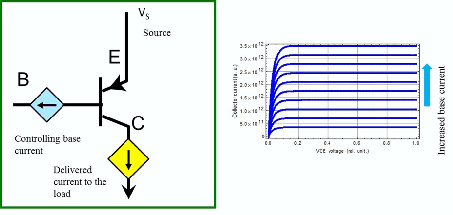
4. I-V curve
4.1 Introduction
BJT is a device where a small current (base)
controls a large current (emitter to collector).
To understand the I-V behavior, we need to calculate the base
current (electron), (which has a specific VEB) and then the
corresponding collector current.
4.2 Base-emitter current
In practice, we control the base-emitter current
with a current source. However, here, we plot the electron
base-emitter current as a function of bias voltage
VEB:
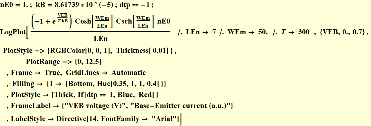
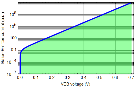
With current source control, we define an inverse function that gives the VEB voltage as a function of the input base-emitter current:
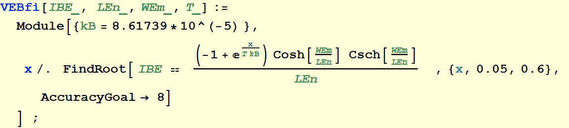
![]()
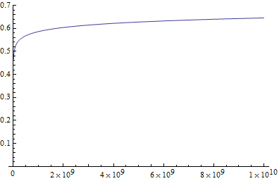
Notice that how the VEB "flats" out with increasing IEB current: because of the exponential behavior: it doesn't take much VEB increase to have a large IEB current
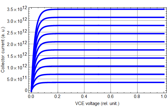
4.3 Diffusion collector current vs. base-to-emitter current
Here, we will see how varying the base current will
affect the collector current:
(the code below may take sometimes to execute, hence please be
patient).
p-n-p transistor IV-curves
Here, we plot the IV family of curve of collector hole current as a function of the emitter-collector bias for increasing base-emitter electron current: this is the transistor action: it is “current switching current”: a little base-emitter electron current can control a large collector hole current: it’s like a lever, or better description: current amplification. This was done with a simplifed approximation that allows faster execution to give the results below.
4.4 Summary on base current
4.4.1 Discussion
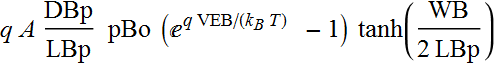
There are 2 main components of base current
1- electron diffusion current from base to emitter (forward diode)
2- electron remobination with the hole current from emitter to
collector that passes through the base.
We can ignore the electron current from collector to base (reverse
diode)
Both of this have been discussed above. Here we put them together:
Component 1:
Component 2
![]() =
= 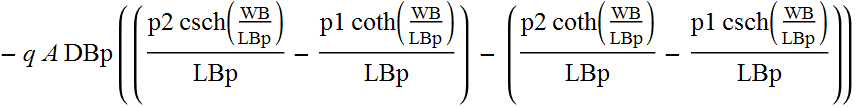
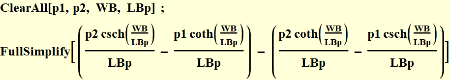
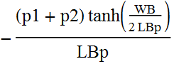
remember that p2 is <<< p1, so the
electron recombination current is ~ 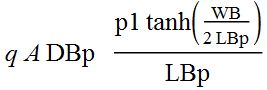 ~
~ 
There are two
components of electron currents: how to reduce each and under
what conditions can they be made small?
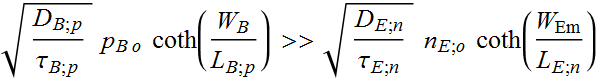
nEo vs. pBo 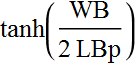 :
very short base to reduce electron recombination current.
:
very short base to reduce electron recombination current.
4.4.2 Summary
To lower the base current, we need:
1- highly asymmetric doping between emitter (heavy) and base
(light) (relative only)
2- long emitter
3- short base