Chapter 5 - Part 1 - Illustration
ECE 4339
Han Q. Le
(copyrighted) U. of Houston
Start package
0. Physical constants or frequently used formulas
Overview
Calculation package
Modules for illustration
Application
1. Review previous p-n junction
1.1 Review homework 3
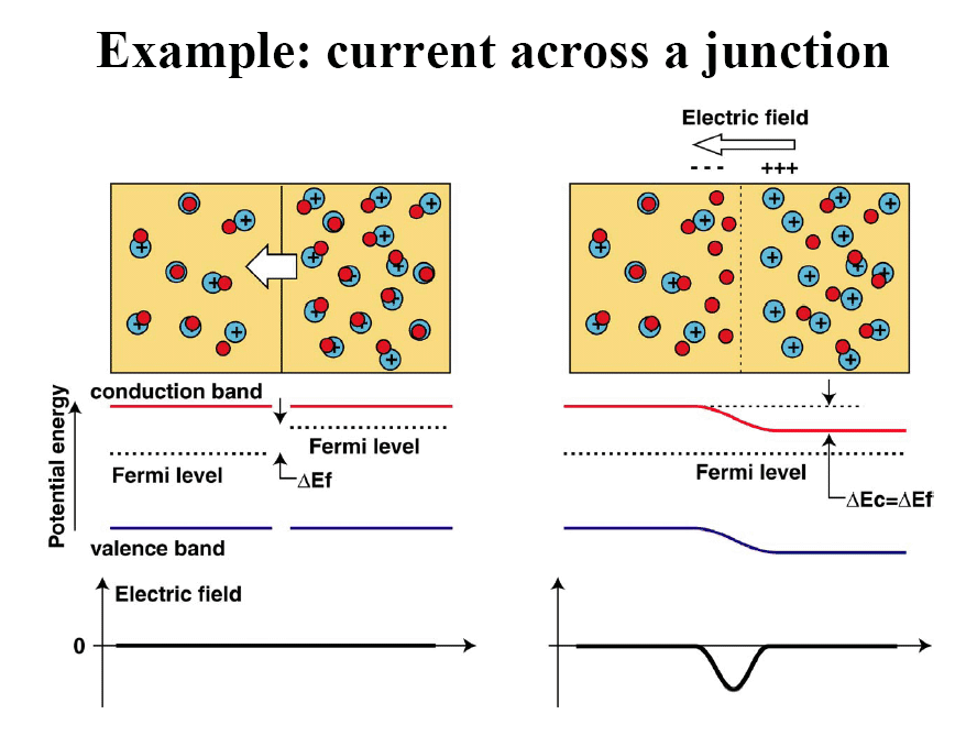
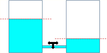
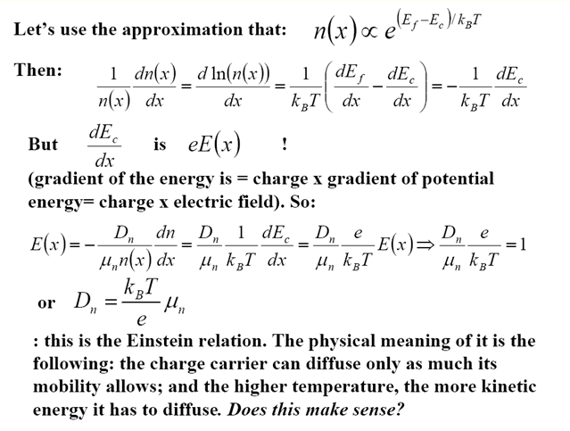
Principle of detailed balancing. If we have the following case:
The left hand side Fermi level is different from
the right. What'll happen?
Carriers diffuse, left goes right and vice versa.
The rate of left going to right = density of occupied states of
left x density of UNOCCUPIED of right:
![]()
Vice versa for the other way and both MUST be equal at equilibrium
![]()
![]()
![]()
We see that this implies: ![]()
What it means is that the Fermi Level must be equal.
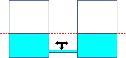
How do they get to the same level?
At -∞ and +∞ we have:
The Fermi levels at -∞ and +∞ stay the
same relative to the band. So, if they level, the band MUST shift
relative to each other. We'll learn how in Chapter 5.

1.2 Diffusion across a junction
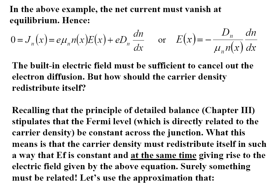
![]() and
and ![]()
Consider just one type of carriers for simplicity.
2. Junction at equilibrium
2.1 Fermi level and contact potential
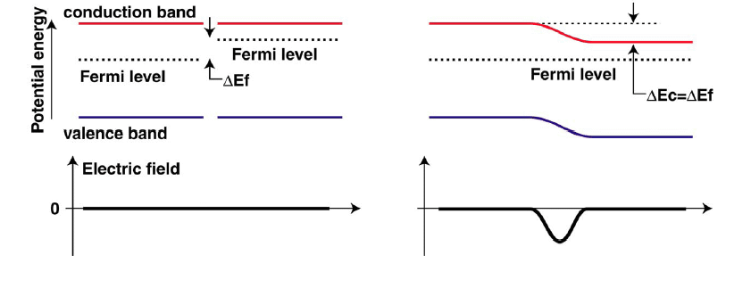
The potential energy shift (caused by internal electric field) is
called contact potential at equilibrium. Example:
Left side is p-doped: ![]()
Right side is n-doped: ![]()
The difference is: ![]()
![]()
2.1.1 Further example
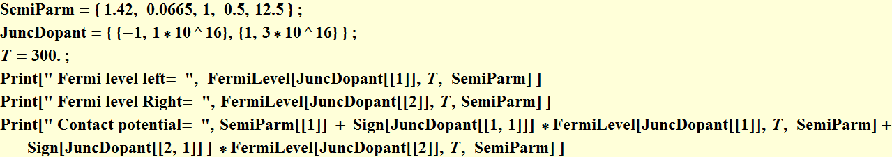
![]()
![]()
![]()
Calculation of Fermi levels
2.2 Carrier distribution
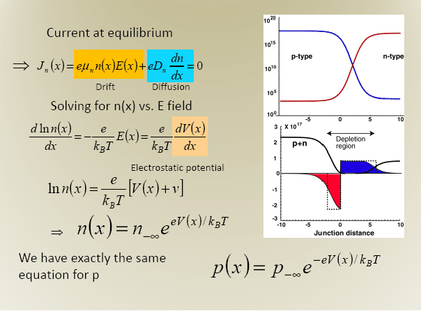

The minimum is at n=p. Total carrier density is LOWEST when there are equal electron and hole population. This is the case of the depletion region
2.3 Depletion layer
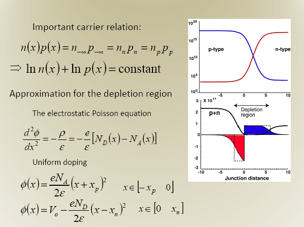
2.4 Electrostatic potential
The electrostatic potential is a function of
contact potential:
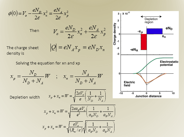
Calculation of static potential energy at the junction
2.5 Illustration a: electrostatic potential
Band diagram at the junction at equilibrium with simplified space charge
2.6 Illustration b: carrier densities
2.6.1 Linear scale
Carrier densities at the junction at equilibrium - linear scale
2.6.2 Log scale
Carrier densities at the junction at equilibrium - log scale
2.6.3 Illustration for junction at equilibrium
Band structure with carrier densities on ![]() scale.
scale.
Band structure with carrier densities on ![]() scale
scale
Band structure with carrier densities on linear scale.
Band structure with carrier densities on linear scale
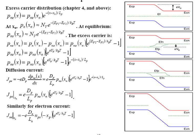
3 Junction under bias
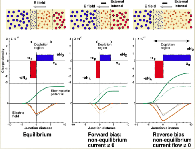
3.1 Junction electrostatic potential
The bias can INCREASE (reverse bias) or DECREASE
(forward bias) the junction electrostatic potential.
The depletion width correspondingly increases or decreases.
In the following,
the convention is that a positive Vbias means forward bias,
negative Vbias means reverse bias. Vbias voltage is NOT relative
with respect to the left side or right side.
Junction electrostatic potential with bias
Band structure with bias
3.2 Carrier density
Reviewing of the diffusion model in Chapter 4
Using the model of diffusion, the carrier excess
density near the junction has the form:
![]() (1)
(1)
We need to find ![]() (2)
(2)
We know
that ![]() (3)
(3)
At equilibrium: ![]() (4)
(4)
Thus: ![]()
![]() (5)
(5)
Subs (5) in (1):
![]() (6)
(6)
Similarly: ![]() (7)
(7)
3.2.1 Excess carrier density under bias: linear scale plotting
Let’s plot excess carrier densities:
Excess carrier densities - linear scale
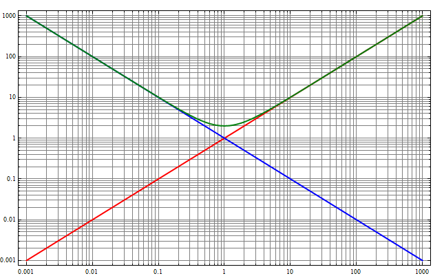
3.2.2 Excess carrier density under bias: Log scale plotting
(positive bias only)
Excess carrier densities - log scale
3.3 Junction diffusion current
Now we can plot the junction diffusion current
using the simple formula:
 ;
; 
3.3.1 Junction diffusion currents: Linear scale plotting
Junction diffusion currents - linear scale
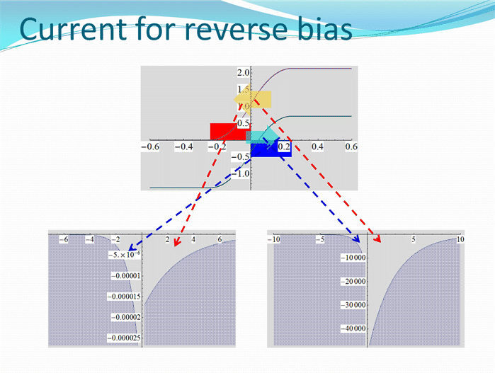
3.4 Diode behavior
The total diffusion current at the junction
is:
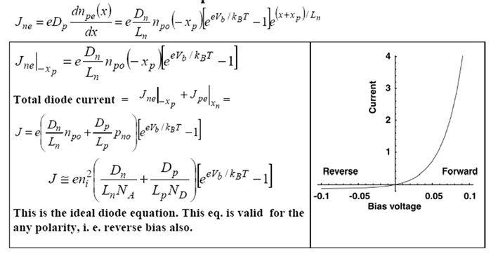
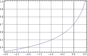
Ideal diode I-V characteristic at low bias and low current density
3.5 Drift and diffusion
Total current is constant every where in the diode.
But diffusion current is not a constant, then what?
![]()
Drift and diffusion currents
4 Junction capacitance
We recall the space charge at a p-n junction:
![]()
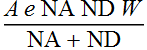
![]()
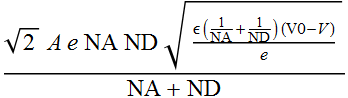
![]()
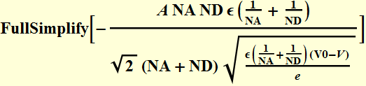
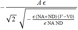
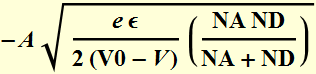

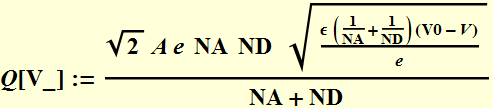
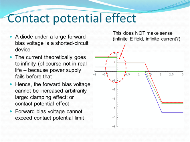
5. Modification of ideal diode behavior
Realistic diode is different from the ideal diode model because of the effect of contact potential. It is given as (See ppt lecture file):
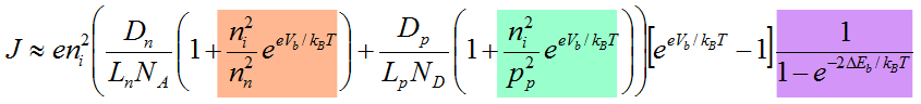
Note the extra term: 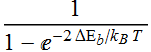 where
where
![]()
What this means is that the bias cannot be greater than the
contact potential because the current would be infinite.
This is the behavior of that term: in essence, it gives “infinite
current” at contact potential bias: the band is completely
flattened out and the whole carrier population contribute to the
current. Of course, this doesnot happen in realistic device
either, because there will be resistivity limit on the drift
current, which is the basic resistance of each segment, p and n.
In real life, the power supply will max out its current output
capability. And if it can give a sufficiently large current that
results in a power exceeding the diode power handling capability,
the diode would be burned up.
5.1 Linear scale plot - see contact potential effect
Modified diode I-V characteristic with contact potential effect - linear scale
5.2 Log scale plot
On log scale we can see the turn-on bias kink when excess minority current is significant before the ultimate limit of contact potential.
Modified diode I-V characteristic - log scale