Chapter 1
ECE 4339-4119 - U Houston
Han Le - Copyrighted
1. Review of resistivity and conductivity
1.1 Resistance & conductance
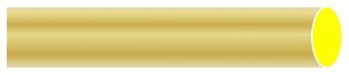
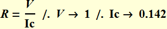
Suppose we have a copper wire. We apply 1 V, and obtain 0.142 A.
1.1.1 Resistance
What is the wire resistance?
![]()
1.1.2 Conductance
What is the wire conductance? Conductance is:  :
:
![]()
![]()
1.2 Scaling the wire dimensions
1.2.1 Scaling the length
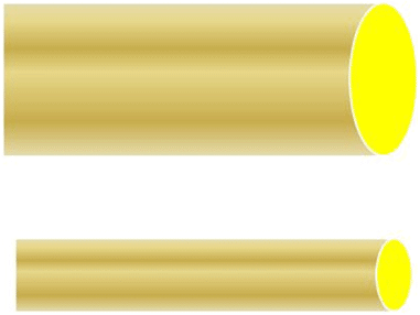
Suppose we double the length of the wire, what will be the resistance?
1.2.2 Scaling the wire cross section
Suppose we obtain a new wire with diameter twice the diameter of the current wire, what will be the resistance?
1.3 Resistivity and conductivity
Current= number of charges passing per unit time.
Analogy: traffic and the road size. What happens when 4-lane
traffic is converted into 2-lane traffic? or vice versa?
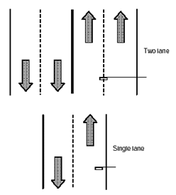
Resistance inversely decreases
as a function of cross section area

If we double the length, each half has only 1/2 voltage, hence,
1/2 the current.
The total resistance is thus doubled.
Resistance increases linearly as a function of length:

There is a coefficient to make the two side equal:

ρ is called the resistivity. It is a property of the material, and
has nothing to do with the length or cross section area of any
particular piece of a material.
A related definition is conductivity, defined as:

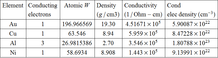
Discussion: fundamentally, what determines the conductivity of a material? (we�ll discuss more in Chapter 3).
From periodic table (example:
http://www.ptable.com/)
Source code: Review of resistance and conductance
Demo: Review of resistance and conductance
Question: what do you think is the reason for semiconductors to have such a wide range of conductivity (but being neither good conductors nor good insulators)?
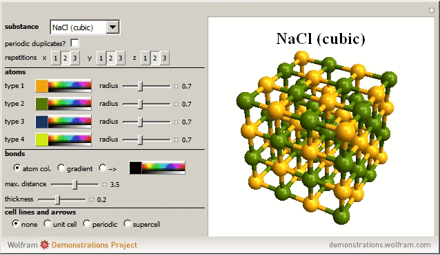
2. Crystal graphics
2.1 Basic crystallography
Demo
http://demonstrations.wolfram.com/SomeRepresentativeCrystalStructures/
http://demonstrations.wolfram.com/CubicCrystalLattices/
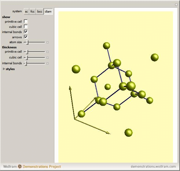
http://demonstrations.wolfram.com/DiamondLattice/
http://demonstrations.wolfram.com/TheStructureOfDiamond/
http://demonstrations.wolfram.com/SpherePacking/
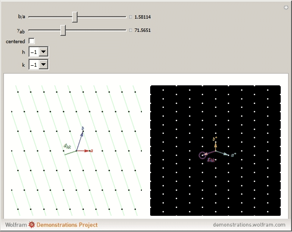
2.2 Crystallographic planes
http://demonstrations.wolfram.com/CrystallographicPlanesForCubicLattices/
http://demonstrations.wolfram.com/MillerIndicesForASimpleCubicLattice/
http://demonstrations.wolfram.com/ReciprocalLattice2D/
http://demonstrations.wolfram.com/GrapheneBrillouinZoneAndElectronicEnergyDispersion/
Homework
Source code: 2D crystal structure
Demo 2D crystal - HW graphene
3. Defect: edge dislocation
http://demonstrations.wolfram.com/MovementOfAnEdgeDislocation/