FET - Summary
Introduction & review
Basic concepts (Review)
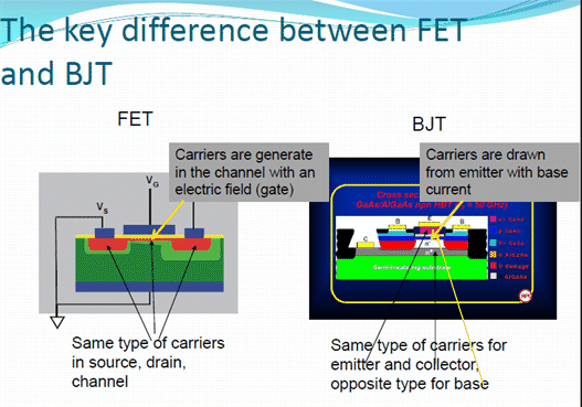
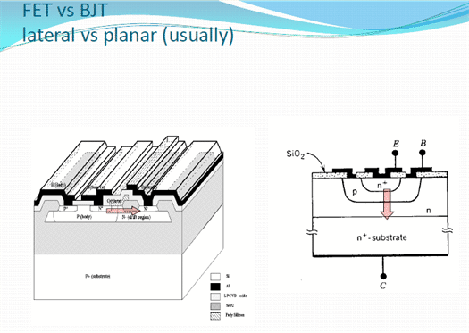
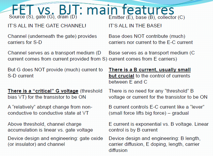
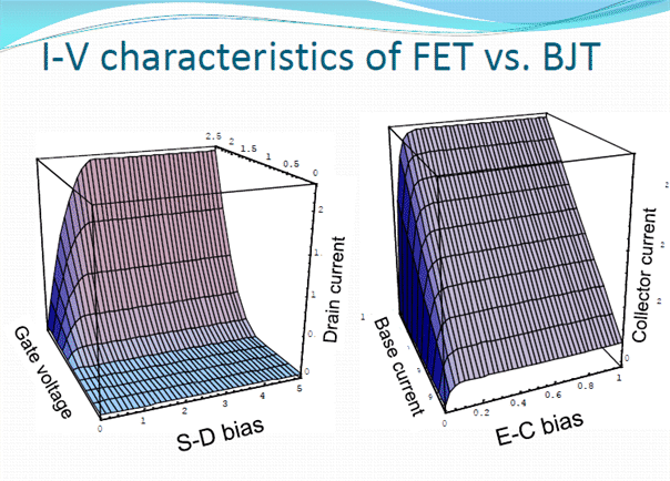
Review the 2 types of transistors
Calculation package
Overview:
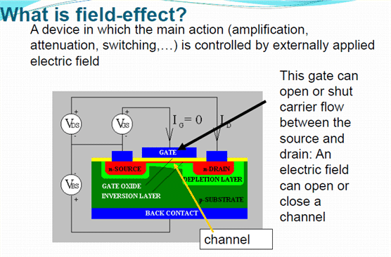
Note: there are many types of FET, for this course,
we need to learn only MOSFET
(MODFET is also useful for FET concept illustration but not
essential).
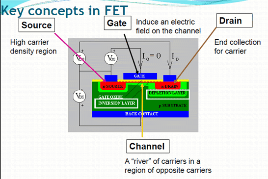
Illustration with two types of FET:
1- Channel normally on: Generic MODFET
- Understand channel pinch-off concept
- Illustration channel current saturation
and IV characteristics
2- Channel normally off: MOSFET
- MOS junction and inversion
- C-V characteristics and switching
efficiency
- IV curve
1. Concept illustration "Generic" FET - MODFET (skip)
2. Element of MOSFET channel: MOS junction, low field and depletion
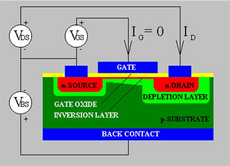
MOSFET:
- Channel normally closed
- Gate voltage is to open (create) channel - A threshold voltage.
- A similar "pinchoff" effect (but a bit more complicated) not
horizontally, but vertically.
- The effect leads to current saturation
2.1 Metal-Oxide-Semiconductor junction
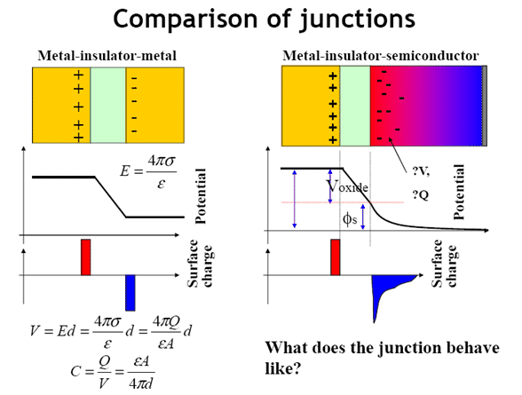
We will see that semiconductor can be:
- insulator-like or very-poor conductor-like
- metal-like
- the transition happens with a �threshold�
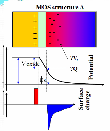
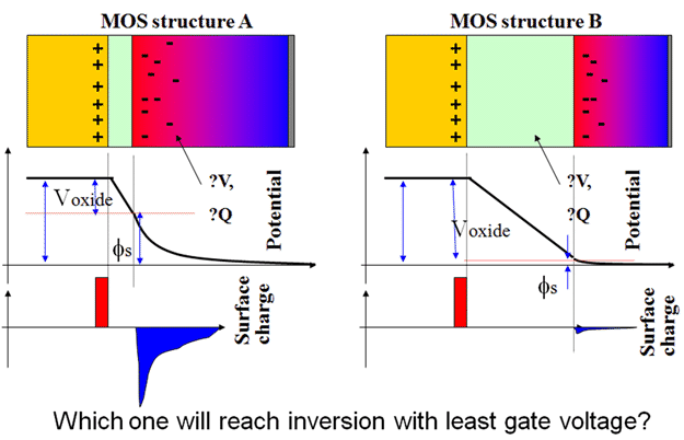
In the illustration below, we see what happens to the charge at the semiconductor junction as a function of gate voltage.
2.2 Band bending and electrostatic
When we apply a field to MOS, what happens in the semiconductor? what is the charge profile in the semiconductor?
We need to calculate the electrostatic potential
and charge density at the channel beneath the oxide (or insulating
layer). V and Q.
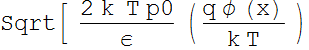
This is done by solving the Poisson's equation.
We will see that there are roughly three conditions:
- low field: charge screening
- stronger field: depletion
- even stronger field: inversion
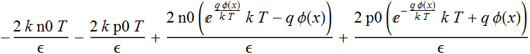
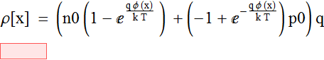
2.1.1 Charge density expression
Charge density is
![]()
At x->∞, the charge is neutral: ie. ρ[x=∞]=0= ![]() -
-![]() +p0-n0)
where p0 and n0 are hole and electron density at equilibrium
(assume ND and NA are uniform). At equilibrium, (see Chapter 3)
+p0-n0)
where p0 and n0 are hole and electron density at equilibrium
(assume ND and NA are uniform). At equilibrium, (see Chapter 3)
![]()
where we denote: ![]()
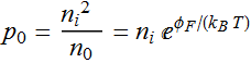
At any point with a potential q
φ[x] added to the band:
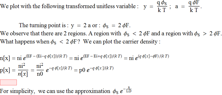
n[x]=ni ![]() =ni
=ni
![]() =n0
=n0
![]()
p[x]=
![]()
![]() =p0
=p0
![]()
Detailed algebra for ![]()
2.1.2 Maxwell-Poisson's equation of electrostatic and charge density (Poisson)
Maxwell-Poisson's equation:
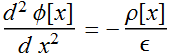
From the detailed algebra result above:
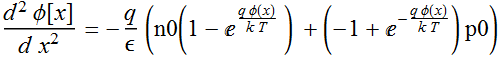
Or:
2
 =-
=-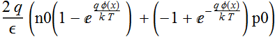

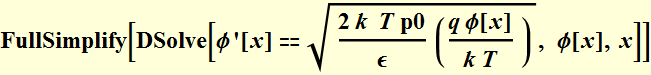
This equation is transcendental and cannot be
solved. But we can get reasonable approximation.
But first, we can to transform it into 1st order differential eq.
for approximation.
Details: transforming into 1st order DE

![]()


Hence, we have a differential
equation:

As mentioned above, this cannot be solve analytically, but can be
approximated for different conditions below.
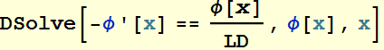
2.3 Approximated solutions for the electrostatic potential: low field
2.3.1 Low field region - detailed algebra
2.3.2 Low field solution
Define  =
= ![]() :
where LD has the unit of length. This is called Debye length, NOT
DIFFUSION length.
:
where LD has the unit of length. This is called Debye length, NOT
DIFFUSION length.
![]()
![]()
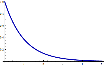
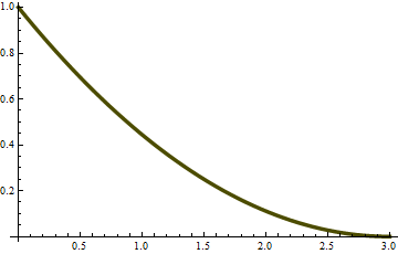
So, at low field, the potential has the exponential
decay profile with a characteristic length LD =  .
LD is called the Debye
length. It signifies the length dimension for which the
charges screen out the potential.
.
LD is called the Debye
length. It signifies the length dimension for which the
charges screen out the potential.
2.4. Approximated solutions for the electrostatic potential: large field region (depletion)
2.4.1 Detailed algebra
Consider now that  is large, >>1 and so
 ![]() is very small, then
is very small, then
 =
= ]
]
![]()
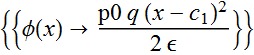
2.4.2 Solution
Hence, the electrostatic is parabolic, similarly to
the depletion regions at a p-n junction, and it is so for exactly
the same reason: depletion of carriers.
![]()

![]()
This is a simple parabolic profile: equivalent with
constant charge. This is the case since by dropping the exponent
term ![]() which represents the charge density variation, the residual charge
must be constant. The charge is:
which represents the charge density variation, the residual charge
must be constant. The charge is:
![]()
Indeed this is similar to what we have seen at p-n junction depletion.
3. Channel inversion
Introduction: Let�s take a look at this:
3.1 Discussion

In the above approximation, the potential is just
that of the constant charge ![]() from doping.
from doping.
But notice something: we always assume that ![]() is very small. If so,
is very small. If so, ![]() is very large and at some point, there is a term that we
neglect:
is very large and at some point, there is a term that we
neglect: ![]() only because the minority carrier concentration
only because the minority carrier concentration ![]() is small.
is small.
At some point, because ![]() is so large,
is so large, ![]() is nolonger negligible, (EVEN as n0 is small as minority carriers)
is nolonger negligible, (EVEN as n0 is small as minority carriers)
To deal with this, we have to
modify our approximation.
3.2 Surface charge density, inversion
The above simple approximation gives us some
insight into the behavior of the MOS junction. With the concept of
Debye length and charge screening, we can rewrite the equation:

= 

We can simplify further by replacing ![]() -->
--> ![]()
We we use Gauss' law, we know that the net charge
accumulation is:
![]() = -ε Efield at the surface. So, the surface
charge is:
= -ε Efield at the surface. So, the surface
charge is:
![]()

q 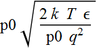

q p0 LD 
Solution is:
We see what happens here:
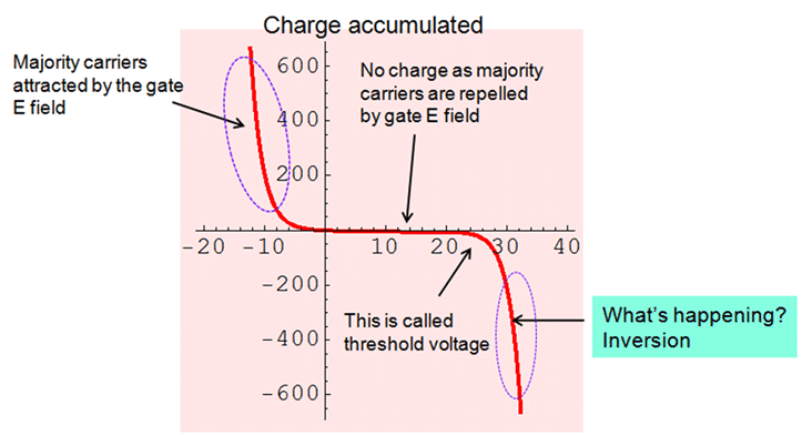
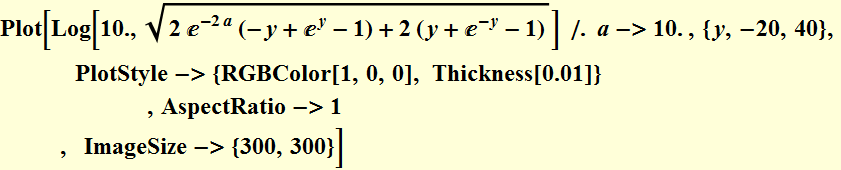
Illustration on log scale
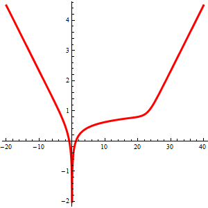
Exercise: where is the majority carrier accumulation? where is the depletion? where is the threshold? and where is the inversion?
3.3 Carrier density (mobile charges)
3.3.1 Illustrations
There are two types of charge (no, not holes
and electrons).
1- fixed charges
associated with ionized acceptors in p-type (or donors in n-type):
these are NOT relevant, because these charges do NOT conduct electricity
2- mobile charges
associated with carriers (either holes or electrons, depending on
the channel type). For the channel, the inversion mobile charge is the key thing that makes a
MOSFET work.
See illustration of carrier density
Illustration of charge density and mobile carrier (electrons) density
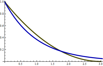
Illustration of hole and electron density on log scale
This is a plot of hole (blue) and electron (red) density on log scale as a function of distance into the semiconductor
The point where carrier type crosses over each other is called the inversion point. The regime where there is a strong electron concentration is called the inversion regime. MOSFET channel is formed by the inversion region underneath a gate.
3.3.2 Net charge density

4. MOS junction C-V and capacitance characteristics
Critical for inversion is the voltage inside
semiconductor.
It is crucial for MOSFET to potential in
semiconductor ![]()
4.1 Capacitance concept
MOS junction is a capacitor. In the above we study
the field (or potential) profile inside the semiconductor.
Externally, MOS can be described interms of capacitance and
accumulated charge
The bias voltage is a sum of voltage across different region:
VB = VOxide + ![]()
VOxide= - where
where ![]() is the charge in metal and semiconductor (equal and opposite
sign).
is the charge in metal and semiconductor (equal and opposite
sign).
Thus:
![]()
But using Gauss' law, we know that:
![]() = ε E[x=0], or = -ε
= ε E[x=0], or = -ε ![]() [x=0]
[x=0]
Thus, the charge balance equation is:
![]() = -ε
= -ε ![]() [x=0]
[x=0]
This is a fundamental relation of MOS junction.:
The full equation is:
![]() =
= 
Or:

See charge plot again:
We can solve the above equation numerically. But it
is more intuitive to see what's going on.
First, we observe that there are 2 types of charges in the
semiconductor. A charge due to the exposed ionized acceptor as the
holes move away from the junction, called depletion charge. The
other is the electrons especially at the inversion. The first
charge is NOT mobile, so they are not contributing to the drain
current. The mobile electron charge is what makes FET work.
From above discussion (Section 2 and the plottings), we see that
charge behavior is quite complicated. There are weak field, strong
depletion, and inversion conditions. Since accumulated charge
behavior directly determines the capacitance, it is clear that the
capacitance of a MOS is very complicated but understanding this
capacitance is essential. In fact, measurement and analysis of MOS
becomes an indispensible tool for experimental characterization of
a MOS channel. Also important is the high frequency characteristic
for fast switching applications.
The differential capacitance is defined as:
![]() =
=  =
=
This is what we need to analyze.
4.2 Depletion region capacitance
For this condition:
![]() ,
where
,
where 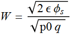 is
a depletion width. But this is practically the capacitance of the
depletion width itself. Hence, the capacitance decreases with
voltage.
is
a depletion width. But this is practically the capacitance of the
depletion width itself. Hence, the capacitance decreases with
voltage.
This is the reason to consider MOS as a series of 2 capacitor: the
oxide and the semiconductor.
The net capacitor is 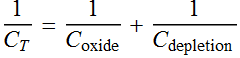
The larger the oxide capacitance, the closer the total capacitance
to  :
more charge for the channel.
:
more charge for the channel.
4.3 Inversion condition and threshold voltage
4.3.1 Discussion
When inversion happens, the mobile electron charge can build up very fast next to the oxide-semiconductor interface. So intuitively, the capacitance must increase again.
The capacitance initially increases with voltage
exponentially. Obviously it can not increase forever. What happens
is that ![]() is "clamped" just above 2 φF so
that increasing the total bias voltage will result mostly increase
in voltage across the oxide.
is "clamped" just above 2 φF so
that increasing the total bias voltage will result mostly increase
in voltage across the oxide.
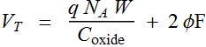
We can write the charge equation as:
![]() =
= ![]() +
+
![]()
where ![]() represents the non-mobile charge of the depletion region, and
represents the non-mobile charge of the depletion region, and ![]() is the electron charge of the MOS channel.
is the electron charge of the MOS channel.
How to express ![]() and
and
![]() ?
?
![]() is the depletion charge: p0 q W =
is the depletion charge: p0 q W = ![]()
By definition: ![]() =
= ![]() -
-
![]() .
.
At the onset of inversion, ![]() -->
--> ![]() ,
and
,
and ![]() -> 2 φF.
-> 2 φF.
We can thus define a bias votage
for the onset of inversion, called threshold voltage:
To see this, let's look at the condition right
around ![]() .
.
4.3.2 Some background algebra (no need to open unless wanting to know details)
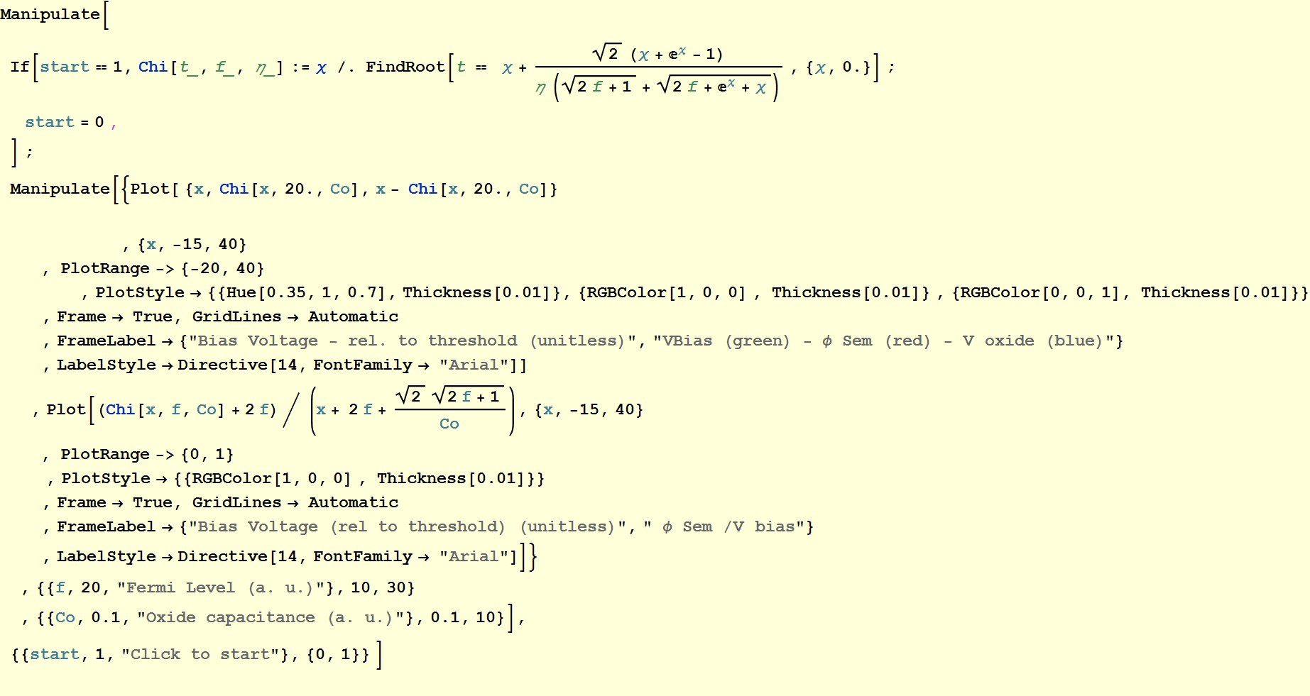
4.3.3 Plot of ![]() clamping and effect of oxide capacitance
clamping and effect of oxide capacitance
We are ready to see the relationship between the oxide capacitance, bias voltage, and bias potential in semiconductor.
To simplify the discussion, we will define the bias voltage ![]() in semiconductor in terms of a unitless quantity:
in semiconductor in terms of a unitless quantity:
![]() or:
or: 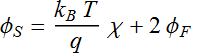 ;
;
It is relative to the Fermi level ![]() .
Remember:
.
Remember: ![]() is simply the Fermi level relative to the intrinsic level and it
is a function of doping.
is simply the Fermi level relative to the intrinsic level and it
is a function of doping.
In turn, we also want to use a unitless quantity for ![]() :
:
 or:
or: 
For capacitance areal density (which is capacitance per unit
area), we use the quantity:
 or:
or: 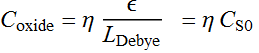 ; we simply define
 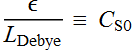 .
.
It is just an quantity that is a property of the semiconductor
having the dimension of capacitance areal density.
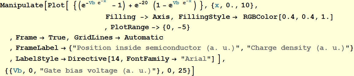
Below is a code to calculate:
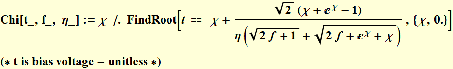
For VB above threshold, ![]() -> 2 φF + small and very slow increase: this is called
clamping. What happens to the rest of the voltage?
-> 2 φF + small and very slow increase: this is called
clamping. What happens to the rest of the voltage?
Critical for inversion is the voltage inside
semiconductor.

4.3.4 Effects of oxide capacitance
One way to think about this is the ratio of  .
.
Obviously, the higher oxide capacitance, the better.
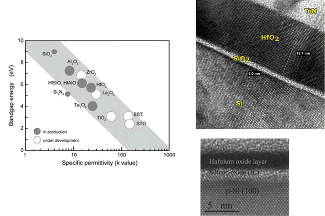
Advanced oxide materials
4.4 Mobile charge
We are interested in the mobile charge, which is what makes the channel to work.
![]()
Illustration of mobile charge density vs gate bias voltage
5. MOSFET simple I-V
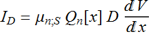
5.1 Basic
If we know the mobile charge ![]() ,
we are ready to find the drain current as a function of gate
voltage and drain-source voltage.
,
we are ready to find the drain current as a function of gate
voltage and drain-source voltage.
What determines the drain current?
In earlier example, we write the voltage-current differential
equation in terms of local resistivity:
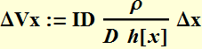
In the example in earlier section, we use a model of MODFET, which allows us to visuallize the change of the channel as a function of gate voltage. It is intuitively easy to comprehend the pinch-off and the channel opeing and closing. BUT the essence of any FET is really in the LOCAL RESISTIVITY, whether the local resistivity is affected by the channel size or by the conductivity DOES NOT matter.
Thus, we can have another perspective of MOSFET by
describing it in terms of conductivity:
![]()
where ![]() is the mobile charge density of the MOS channel as discussed
above.
is the mobile charge density of the MOS channel as discussed
above.![]() is the channel carrier (n-type) mobility in the channel, which is
at the interface beween the gate and the oxide. D is the effective
channel depth, which, for simplicity, we approximate as a
constant. (Discussion in class about modification to this
approximation). We do not need to specify channel width and the
current is implicitly the current density per unit of channel
width.
is the channel carrier (n-type) mobility in the channel, which is
at the interface beween the gate and the oxide. D is the effective
channel depth, which, for simplicity, we approximate as a
constant. (Discussion in class about modification to this
approximation). We do not need to specify channel width and the
current is implicitly the current density per unit of channel
width.
![]()
To solve this equation, we need a relation between ![]() and ΔV[x].
and ΔV[x].
Both ![]() and
and ![]() are functions of (
are functions of (![]() - V[x]).
- V[x]).
![]()
![]()
5.2 Simple plot
The channel is functional above threshold voltage.
At that point ![]() ~ 2
~ 2 ![]() . But we recall the definition:
. But we recall the definition:
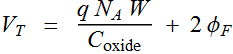 for V threshold,
where  ~
~ ![]() ,
and 2
,
and 2 ![]() ~
~ ![]() ,
the charge equation can be written:
,
the charge equation can be written:
![]()
Or:
![]()
Hence:
![]()
We can integrate both sides:
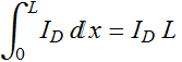
and:
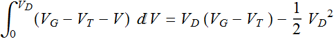
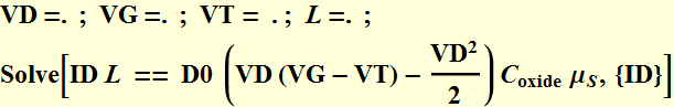
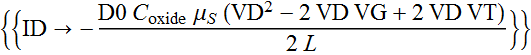
Or: 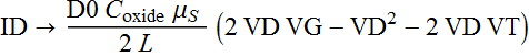
and  is defined as the transconductance
![]() .
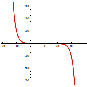
Saturation of drain current occurs when d ID/d VD =0:
.
Saturation of drain current occurs when d ID/d VD =0:
![]()
![]()
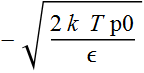
Notice the similarity of VT and VPO in the generic FET.
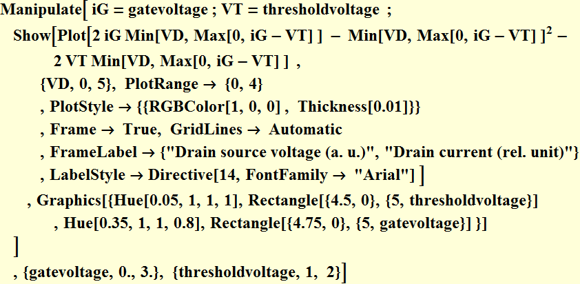
Now, we can plot

![]()
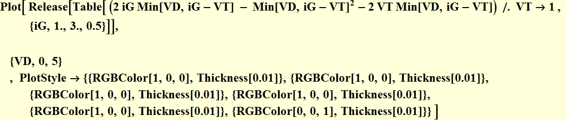
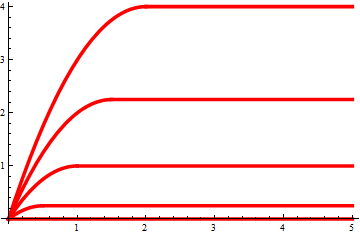
We see that this model gives the same I-V characteristics of typical FET or transistor.