Homework 4 A
ECE 4339 Spring
2014
Han Q. Le
(copyrighted) U. of Houston
Part A
1. (20 pts)
Watch the following:
https://www.youtube.com/watch?v=tg3SyGHilaQ
https://www.youtube.com/watch?v=5z4HbRc0YNY
https://www.youtube.com/watch?v=uze7ZTT3E0A
Write a 2-page report (12 pt font, single space) of what you
observe and learn from these videos about Si technology with
regard to device fabrication:
lithography, doping, device structure. Do not write the
parts about technology for social use (at the beginning), or about
logical devices etc.
There are many other similar videos (example:
https://www.youtube.com/watch?v=UvluuAIiA50). Feel free to watch
them and synthesize your
knowledge to write the report. Remember, this is not a
narrative of what you see like watching a TV show or a movie. This
is about synthesizing what you observe and learn into knowledge
and write as if you are explaining to someone who doesn’t know or
have the opportunity to watch them. Do not read or copy
figures, materials elsewhere and insert in your paper. (You can
read on your own for further understanding if you are interested).
This is about watching, taking
notes, synthesizing and reporting what you learn.
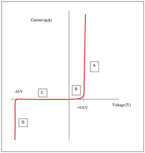
2. (20 pts) Turn-on voltage for different semiconductors
We remember “the rule of 0.6 V” for diode.
If we have semiconductors of different bandgaps, is
the same 0.6-V-rule applied?
Do the follow. Use the result of Chapter 5-Part 1, section 5.2.
Below is the default plot for a GaAs symmetric diode with ![]() doping concentration
on both sides.
doping concentration
on both sides.
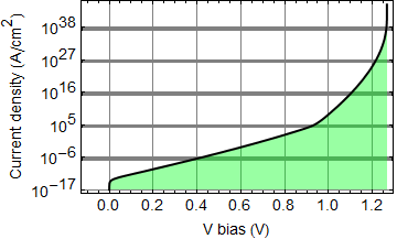
2.1 (5 pts)
Estimate the values of the “turn-on” voltage (the kink between 0.9 - 1 V) and the ultimate contact potential (where the band diagram is completely flattened out) for this GaAs structure.
2.2 (5 pts)
Obtain a plot and do the same as in 2.1 for Si (look up parameters for Si)
2.3 (5 pts)
Obtain a plot and do the same as in 2.1 for GaP (for this, use gc=1 and effective DOS electron mass 0.79 and effective DOS hole mass 0.83; look up all other parameters for GaP)
2.4 (5 pts)
Make a table comparing all three semiconductors with a column for band gap, turn-on voltage, and contact potential. What do you conclude on the relationship between the turn-on voltage, contact potential vs. bandgap.
3. (60 pts) A structure with 2 junctions (bipolar-junction-transistor-like)
You will need to look up the right parameters for Si (cf. chapter 3) for this problem. Do not worry about getting “exact” values, because different sources may have the parameters slightly different. Obtain from some credible sources and make a reference. Make sure you explitcitly list all the relevant parameter you use for the problem.
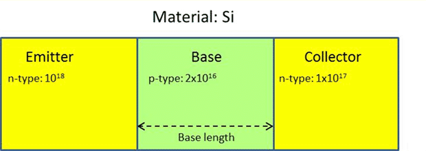
Consider the structure above. The temperature is T=300K.
3.1 (10 pts)
Draw the band diagram with space charge and depletion region for the E-B junction at equilibrium (zero bias voltage between E-B). Do not include the carrier density. (remember, E on the left, B on the right)
3.2 (10 pts)
Draw the carrier density on log scale for the condition in 2.1, and place it directly underneath the figure obtained in 2.1 (this is a separate question. DO NOT draw a single diagram and claim it is for both questions 2.1 and 2.2 - you can duplicate the figure in 2.1 and put it above the figure for carrier density)
3.3 (10 pts)
Draw the band diagram with space charge and depletion region for the B-C junction at equilibrium (zero bias voltage between E-B). Do not include the carrier density.
3.4 (10 pts)
Draw the carrier density on log scale for the condition in 2.3, and place it directly underneath the figure obtained in 2.3
3.5 (10 pts)
Let the base length = 50 μm. Draw two plots: Top:
the band diagram of the entire structure, bottom: the carrier
density profile of the entire structure on linear scale.
It is OK to lose resolution of the depletion region of each
junction because they are very small on the scale of Base length.
3.6 (10 pts)
In the plots of 3.5, you will see that there are a
lot of electrons in the emitter. If we apply a bias between
collector and emitter, it is reasonable to expect electrons to
flow from emitter to collector. But we will find out (in Part B)
that the current is insignificant.
a- What prevents electrons in the emitter to migrate to the
collector? (Think of high level water on one side of a reservior,
what prevents the water to flow into a low-level down stream
lake?).
b- What can you do to make the current flow from left to right
with significant current density?