Homework 4 B
ECE 4339 Spring
2014
Han Q. Le
(copyrighted) U. of Houston
Part B
4. (50 pts)
This problem involves the same structure as in Part A, prob. 3. The Base length is 50 μm. We now apply 3 V between Collector and Emitter. (C is higher voltage than E). No voltage is applied to the Base, i. e. it is floated (No voltage does not mean zero voltage).
4.1 (10 pts)
What do you think the current and band diagram are like. First, hand sketch (or draw with computer programs such as ppt or paint or any graphics package) what you think the band diagram should look like (use the result in Prob. 3). Then discuss in plain English what the current should be (for simplicity, just assume the structure has uniform cross section, hence, the same current flows through 3 regions: E-B junction, along the Base, and B-C junction. (this part is about analytical thinking).
4.2 (30 pts)
We can solve the question in 4.1 more
quantitatively by doing the follow: Let the current be ![]() . we can plot I-V curve
for each segment:
. we can plot I-V curve
for each segment:
4.2.a (10 pts) EB junction
Its voltage is ![]() (obtained by the
inverse of I-V) (we just plot the current density and not worry
about the actual cross section)
(obtained by the
inverse of I-V) (we just plot the current density and not worry
about the actual cross section)
4.2.b (10 pts) Along the length of the Base
The Base is long, hence, we should not assume that
there is no voltage drop from one end to another, although as we
will findout, it is small - but we must show it). The voltage is ![]() where R is the
resistance.
where R is the
resistance.
4.2.c (10 pts) BC junction
Its voltage is ![]()
If we plot all three, we have to find a common
value ![]() such that:
such that:
![]()
We can use graphical technique to solve this
equation. Approximation is acceptable, because you will see that
the current is really limited by just one of the three above (you
have to find out which one), and most of the voltage drop is
across that part. Hence, you obtain ![]() .
.
4.3 (10 pts)
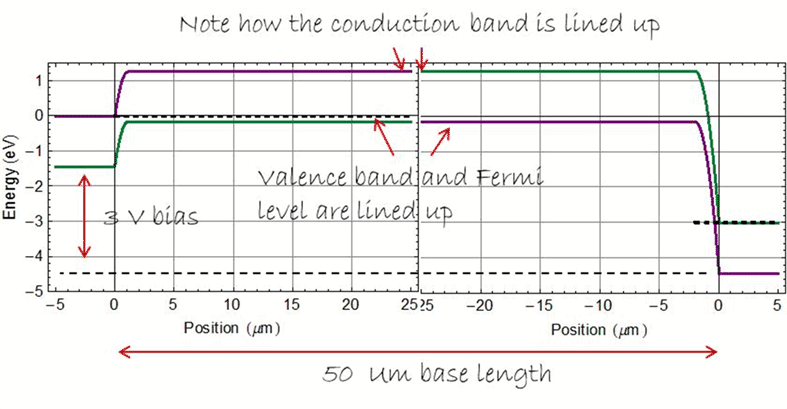
Plot the band diagram of the entire structure using
the value of ![]() obtained above. For
simplicity and since
obtained above. For
simplicity and since ![]() is small we can just
let it be 0. Plot the excess carrier density (on linear scale).
is small we can just
let it be 0. Plot the excess carrier density (on linear scale).
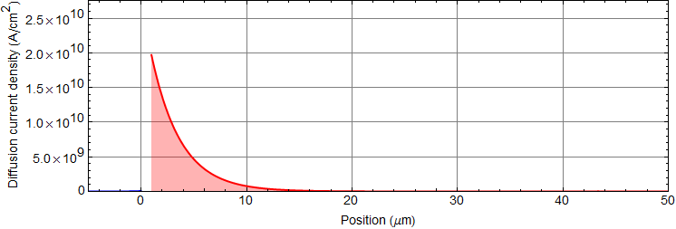
Below is the example for GaAs, not Si which is what you have to do. It is shown here only to give you a rough idea. Delete it and do NOT include in your work. It is ONLY an example.
5. (50 pts)
This is about the same structure in problem 4. (You must finish Prob. 4 first)
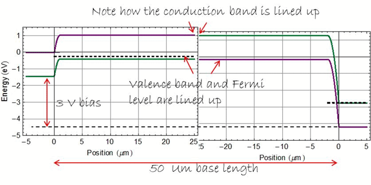
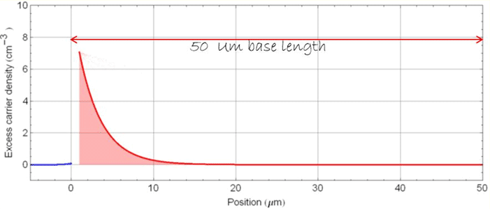
5.1 (20 pts)
Apply -0.25 V between E and B, while maintaining -3
V between E and C (what is the voltage between B and C?). Plot the
band diagram of the whole structure, the carrier density, and the
diffusion current between E and B on linear scale in a vertical
column with properly aligned horizontal axis (see example below).
Use the following value of diffusion lengths (these values are not
correct for Si, but we use it just to illustrate the idea): ![]() ,
, ![]() .
.
Below is the example for GaAs, not Si which is what you have to do. It is shown here only to give you a rough idea. Delete it and do NOT include in your work. It is ONLY an example.
5.2 (10 pts)
Analyze results you obtained in 5.1. By applying a
forward bias voltage 0.25 V between E and B, it is equivalent with
“lowering the dam” to let the electrons (water) from the Emitter
to flow through the Base (water flows over the lowered dam) and
into the Collector. However, are there really a lot of diffusing
electrons (this is a qualitative statement) from Emitter reaching
the Base-Collector junction? would you estimate it at less than
1%? (calculate and explain your answer).
If all things are the same, you cannot change anything except for
the dimension of the structure, what would you change to allow
more Emitter electrons to reach the Collector?
5.3 (20 pts)
Do the same as in 5.1, except that the Base length now is 5 μm. Compare with your analysis of 5.2, are there alot of Emitter electrons reaching the Collector here? How much?