

|
ECE 2100 Lab. V -
Capacitors and RC Circuits
Please
download these
items:
1. Lab 5 workbook and report 2. ECE_2100_Lab_5_guide_Part_0 ECE_2100_Lab_5_guide_Part_A ECE_2100_Lab_5_guide_Part_B_C ECE_2100_Lab_5_circuit_simulation |
Update page b
| Lab
work modification: TBD
(after class survey and Lab
4) |
Part C - Integration circuit
Step C.1: This circuit is very tolerant. When building the circuit, use the closest components you have to the nominal values. Even if it is off by a factor of 2 or more, because it is low-pass, the frequency range of interest will never exceed the op amp bandwidth, and the basic behavior, i. e. the first-order response will always be there for studying. Enter your values in the circuit simulation app
Step C.2: The most basic test of integration (and most common in applications) is to get a linear slope output with a constant input. Hence, the basic test is to use a square wave to obtain a saw tooth or triangle output. One very simplistic illustration is the simulation of CTIA in Step C.3. Make sure that if you have a serious large DC offset problem, use AC coupling output.
Step C.3: ?
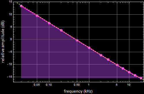
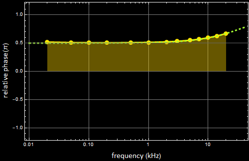
Step C.4: See below for actual data of the circuit in the photographs on page 4.
The points and the solid curves are experimental data, and the dashed curves are the model fit.
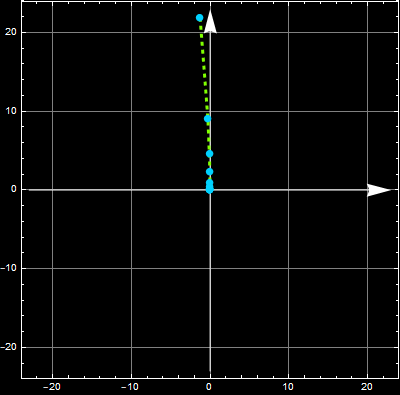
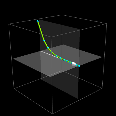
Below are Nyquist plot 2D and 3 D
Step C.5: ?