

|
|
ECE 2100 Lab. IV -
Dependent Sources -
Operational Amplifier
Voltage Amplifier, Transimpedance Amplifier Please
download these
items:
1. Lab 4 workbook and report 2. ECE_2100_Lab_4_guide_Part_0 ECE_2100_Lab_4_guide_Part_1 Special guide: ECE_2100_Lab_4_CircB_wiring_guide Special guide: ECE_2100_Lab_4_Part_1_Step_5_AD2_guide ECE_2100_Lab_4_guide_Part_A
ECE_2100_Lab_4_guide_Part_B
and C
see demonstration and write a report only) Continued from page 2 |
Page 3
Please go to update pages for the latest modification, class-wise issues, and others if links for those pages exist.
update page a update page b update page c
|
Lab work modification: - Do Part 0 ( Introduction), Part 1 (Instrumentation), and Part A only (three parts total): do everything, including answering/discussion all questions.- Experimental work of Part B and C are not required: It means no circuit, no measurement needs be done. You are required to only observe and write a report of your understanding, thoughts, and summary of these Parts. This should be put at the end of your report, a synthesis of everything that you learn in Lab 4. Create a subsection, titled "Report on observation of Parts B and C demonstrations". Do not mix this with what you summarize for your work in Part A. However, if you do anywork along the line of Part B and Part C, you are welcome to include for extra credit. |
Lab work (continued):
Circuit
A
Before
you start:
- handle the photodiode with a pair of
needle-nose pliers or tweezers, grabbing
its legs or the side. Avoid using your
bare fingers as much as possible, and do
not touch the top surface (light sensitive
region), especially the small wire
(~250-um diameter) that connects the top
layer to one of the electrodes.
- identify the cathode,
which has a marker on the leg, a notch, or
a dark line on the light-sensitive
surface. Look at the spec
sheet for details, also this
figure.
- critical: apply
POSITIVE bias voltage to the cathode;
this is known as REVERSE
bias, which is OPPOSITE to forward bias
in the case of LED. Please
do not ever forward bias your photodiode.
- photodiode is a delicate device. Think
of it like your eyes. Some of the maximum
ratings from the spec sheet are shown
below:
- For forward bias (if accidental)

At a mere 1.3 V forward bias, the device
already draws 100 mA, which means 130 mW.
As one can see in the below, the maximum
power dissipation is 150 mW. If you
accidentally connect the 15 V power supply
to its anode, it would likely draw several
hundred mA for a fraction of a second,
heated up quickly, and will be
subsequently degraded or damaged.
- For reverse bias and maximum power dissipation

Since we use only +15 V max, we don't have
to be concerned with the 32-V limit. The
light level we apply will be in the range
of uW or << 1 mW, hence, the
photocurrent will be << 1 mA and we
need not be concerned with the 150-mW
power limit. However, as discussed above,
forward bias will result in ~ or > 150
mW, which will cause degradation or damage
to the device.
We do have a few spares and you can ask
for another one, but it is best if you can
avoid this mistake from the beginning.
-if you are curious, read the below if you
wish to know the most relevant reason why
we must use in reverse bias voltage (look
under the topic of dark-current shot
noise).
- introduction to photodetectors, part 1
- introduction to photodetectors, part 2
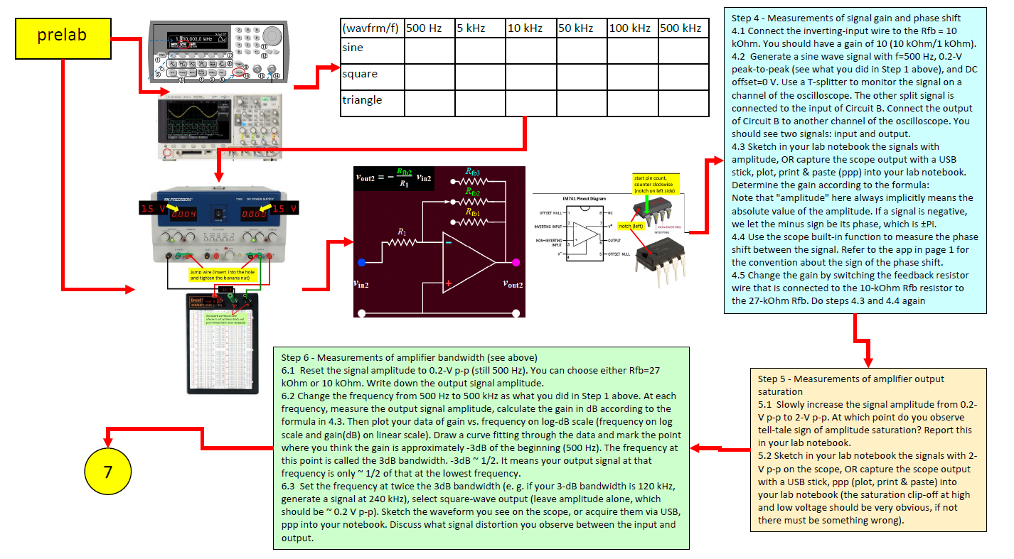
Step 7 - Build Circuit A (see page 1)
Make sure you read through the above.
Do not turn on your power supply until you finish and double check on the wiring.
7.1
Choose the feedback resistor R0 = 10
kOhm to start. Later, if you see
Circuit B output saturated at 14-dB
gain (x27) with moderate light level,
you can select a lower value, such as
2.7 kOhm.

7.2
Connect +15 V source (in off-state) to
the photodiode cathode (very important - do
not make mistake of its
polarity, this is called
reverse bias). The
anode is connected to the op-amp
inverting input. Note: in all
photodiodes, the cathode side always has
a marker, which can be a tag (a little
ear), a spur or a notch, depending on
the package. It also comes in with a
shorter leg than the anode, however,
just in case the legs of a photodiode
might have been modified for soldering
or whatever, identify the cathode by the
marker.
Below is an illustration, your
photodiode may or may not look identical
to this, but the method of marking of
the cathode is the same.
notice the notch on the
right side? That's the cathode, where
+15 V goes to. (you can also
tell by the wire contact at top. The
majority of commercial silicon PIN PD
are grown on n+ substrate, which means
p-layer (or p-type or anode) is on top
and hence you might see the ohmic
contact wire on the anode side - be
very careful not to touch it, the wire
is delicate in an exposed
package. In the future, we will purchase
PD in a TO can with protective cover,
but for now, please be careful).
7.3 Put a
light-shield enclosure over the photodiode
as instructed
previously.
7.4 Connect the output of Circuit A
to the input of Circuit B like the above
(you can choose the Rfb of Circuit B to be
100 kOhm for maximum gain to start, later
you can change to any other Rfb
to have your signal
amplitude in the ~0.1-few V range).
7.5 Turn on the power supply, look
at output vout2 on the oscilloscope, you
may see the high-frequency modulation of
the room fluorescent light that leaks
through the light shield. Move your hand
back and forth over the PD enclosure
aperture. You should see signal responses.
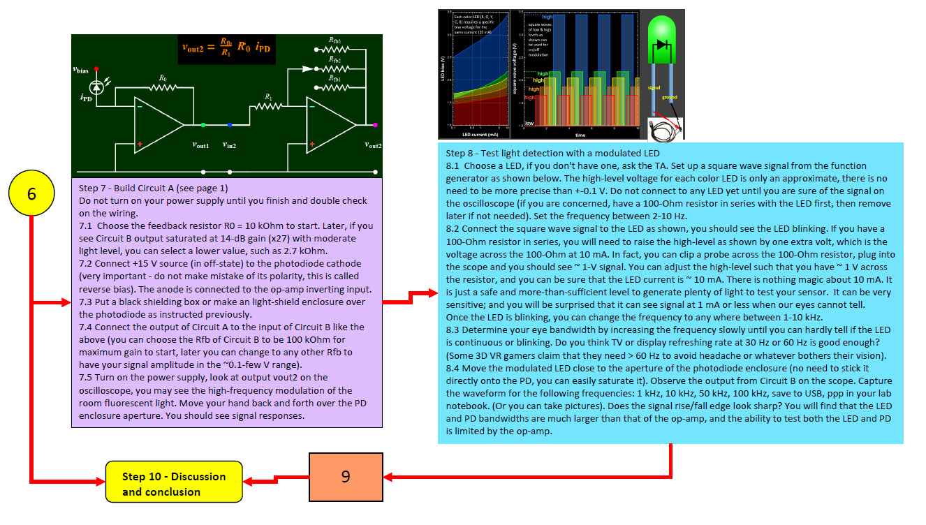
Step 8 - Test light detection with a modulated LED
8.1 Choose a LED, if you don't
have one, ask the TA. Set up a square wave
signal from the function generator as
shown below. The high-level voltage for
each color LED is only an approximate,
there is no need to be more precise than
+-0.1 V. Do not connect
to any LED yet until you are sure of
the signal on the oscilloscope
(if you are concerned, have a 100-Ohm
resistor in series with the LED first,
then remove later if not needed). Set the
frequency between 2-10 Hz.

8.2
Connect the square wave signal to the
LED as shown, you should see the LED
blinking. If you have a 100-Ohm
resistor in series, you will need to raise
the high-level as shown by one extra volt,
which is the voltage across the 100-Ohm at
10 mA. In fact, you can clip a probe
across the 100-Ohm resistor, plug into the
scope and you should see ~ 1-V signal. You
can adjust the high-level such that you
have ~ 1 V across the resistor, and you
can be sure that the LED current is ~ 10
mA. There is nothing magic about 10 mA. It
is just a safe and more-than-sufficient
level to generate plenty of light to test
your sensor. It can be very
sensitive; and you will be surprised that
it can see signal at 1 mA or less when our
eyes cannot tell.
Once the LED is blinking, you can change
the frequency to any where between 1-10
kHz.
8.3 Determine your eye bandwidth by
increasing the frequency slowly until you
can hardly tell if the LED is continuous
or blinking. Do you think TV or display
refreshing rate at 30 Hz or 60 Hz is good
enough? (Some 3D VR gamers claim that they
need > 60 Hz to avoid headache or
whatever bothers their vision).
8.4 Move the modulated LED close to
the aperture of the photodiode enclosure
(no need to stick it directly onto the PD,
you can easily saturate it). Observe the
output from Circuit B on the scope.
Capture the waveform for the following
frequencies: 1 kHz, 10 kHz, 50 kHz, 100
kHz, save to USB, ppp
in your lab notebook. (Or
you can take pictures). Does the signal
rise/fall edge look sharp? You will find
that the LED and PD bandwidths are much
larger than that of the op-amp, and the
ability to test both the LED and PD is
limited by the op-amp.
Step 9 - Test light detection with your remote control
This is not required, but you will get extra 20 points if you can point the remote control toward the PD enclosure aperture and capture the communication signals (set up positive edge trigger and save). Think of it like the remote control "texting" your TV, telling it what to do. The signal consists of a carrier, which is a square wave of ~ 40 kHz, superimposed by the digital "texting signal."
Below are examples.
| This is the "texting"
message: the codes consist of bit 0
and 1 superimposed on the carrier
wave on the right. If you capture
something like this, you will get
extra credit. You see that the
communication rate is ~ 4 bits/2.5
ms, or ~ 1.6 kb/sec |
This is a zoom-in of
the signal on the left, showing
square wave at 37.04 kHz. This is
the carrier wave. |
Feel free to perform any other test that you can think of, beyond the remote control. For example, if you have a mechanical rotary device, like a small fan (such as a computer fan), or the rotor blade of a drone, you can measure its frequency by letting the blade chop a continuous LED beam, or even ambient light. Optical measurement is considered to be the best method in terms of sensitivity and accuracy to study most mechanical phenomena, and widely used in research and industry. Do experiments that interest you. If it is relevant and demonstrates your learning, you will get extra credit.
(You can watch the video below to get your idea. Your optical sensor can be used to detect the light scattered from an object like the video).
Step 10 - Discussion and conclusion
Discuss the research questions. Cite your data as evidence to support your points. Below is some "food for thoughts" guidance, something that we can think about: Is this model of the circuit absolutely correct?
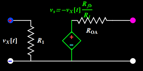
The answer, as we see, is "sort of", but "no": vs[t] cannot be instantaneously proportional to vX[t]. Review your square wave data. If some entity, such as vX[t] depends on another entity vs[t] as cause-and-effect, then there must be mechanism for time delay, because nothing is transmitted instantaneously in the Universe. The time-delay effect can be observed at the leading edge or trailing edge or both when the input changes so fast that it is "instantaneous." We discuss this in the introduction as well. For those who have learned phasor and Fourier analysis, it means that the response cannot be the same for all frequencies. In fact, the whole Step 6, especially 6.2 is about the frequency-dependence effects. Hence, it is more appropriate to express the op amp circuit in the frequency domain:
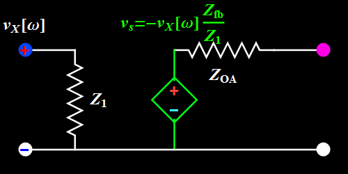
In this figure, vX[omega] is the input phasor. See the app for phasor concept. vs is the output phasor, which may have a different amplitude and phase than those of the input. Ratio Zfb and Z1 is a complex number that represents that amplitude and phase difference.
Here, the various resistances become complex impedances that implicitly contain the finite-time-response property of the op amp.
The above discussion is for your learning. You don't have to understand if it is beyond what you have learned. But it is an introduction to things that you will learn later in more advanced courses. Hence, you should feel free to express your thoughts, do not feel as if there are certain correct answers and try to guess how to answer them. This is your work, your research, and this last part is to synthesize your knowledge. If you do Circuit A as well, and learn something interesting from your results, such as certain properties of the harmonics of your drone blades, or some objects you like etc., feel free to report and write what interests you and why.
Appendix Quick Lab flowchart
continue to appendix - page i